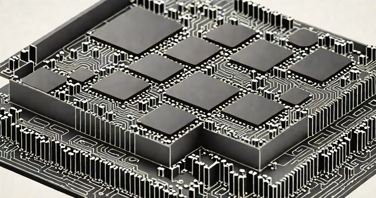
N-type semiconductors are materials with added impurities-typically pentavalent elements like phosphorus or arsenic-that donate extra electrons, increasing electrical conductivity. These materials form the foundation of diodes, transistors, and photovoltaic cells.
When pure silicon is doped with phosphorus, each phosphorus atom replaces a silicon atom in the crystal lattice. Phosphorus has five valence electrons, while silicon has four. The fifth electron is loosely bound and easily freed at room temperature, becoming a mobile charge carrier. This creates an excess of negative charge carriers-electrons-giving the material its name.
The process is called extrinsic doping. Unlike intrinsic semiconductors, which rely on thermally generated electron-hole pairs, n-type materials conduct electricity primarily through electrons. This makes them ideal for applications requiring fast electron movement, such as in logic gates and high-speed switching circuits.
Electrical conduction in n-type semiconductors occurs via electron drift under an applied electric field. When voltage is applied across a doped silicon sample, the free electrons move toward the positive terminal. This flow constitutes current.
At absolute zero, all electrons remain bound to their atoms. As temperature increases, thermal energy frees some electrons from donor atoms (like phosphorus), creating mobile charge carriers. Even at room temperature, enough electrons are available to support significant current flow-far more than in undoped silicon.
For example, a 1 cm³ piece of silicon doped with 1 part per million (ppm) phosphorus contains about 5 × 10¹⁶ phosphorus atoms. Each contributes one free electron, resulting in roughly 5 × 10¹⁶ mobile electrons per cubic centimeter. This density is sufficient to achieve conductivity levels thousands of times higher than pure silicon.
N-type semiconductors are most commonly made from silicon, but germanium and gallium arsenide are also used in specialized devices. The choice depends on bandgap energy, electron mobility, and application requirements.
| Material | Dopant Example | Bandgap (eV) | Typical Use |
|---|---|---|---|
| Silicon | Phosphorus, Arsenic | 1.12 | Integrated circuits, solar cells |
| Germanium | Arsenic | 0.67 | Early transistors, infrared detectors |
| Gallium Arsenide | Silicon (substitutional) | 1.43 | High-frequency devices, LEDs |
Phosphorus is preferred in silicon because it diffuses well during fabrication and forms stable bonds. Arsenic is used in high-performance devices due to its higher solubility and lower diffusion rate, reducing unwanted spreading during processing.
One key distinction often missed: n-type doping does not create holes. Hole conduction is exclusive to p-type materials. In n-type semiconductors, holes exist only as minority carriers-created thermally-and are negligible compared to the abundance of electrons.
Many assume that adding dopants simply increases "charge" in a material. That's incorrect. Doping doesn't add net charge-it introduces mobile electrons while maintaining neutrality. The donor atom becomes a positively charged ion after losing an electron, but the lattice remains balanced.
Another misconception is that n-type semiconductors are always negatively charged. They are electrically neutral. The term "n-type" refers to the majority charge carrier being negative (electrons), not the material's charge.
A less obvious point: the Fermi level in n-type semiconductors lies close to the conduction band. In intrinsic silicon, the Fermi level sits near the middle of the bandgap. After doping, it shifts upward-closer to the conduction band-indicating a higher probability of finding electrons in the conduction band even at low temperatures.
N-type semiconductors are essential in modern electronics. The most common application is in junctions with p-type materials-forming p-n junctions. These junctions are the core of diodes and transistors.
Consider a silicon-based solar cell. The top layer is doped with phosphorus to form an n-type region. Light photons excite electrons in the silicon, creating electron-hole pairs. The built-in electric field at the p-n junction separates them: electrons move toward the n-side, holes toward the p-side. External circuits collect this current, generating usable power.
In a CMOS transistor, the source and drain regions are heavily doped with phosphorus to create n-type contacts. When a voltage is applied to the gate, it forms a conductive channel between source and drain. This enables switching in microprocessors and memory chips.
I once observed a silicon wafer during a cleanroom fabrication run. A 200 mm wafer was exposed to phosphorus gas at 1000°C for 30 minutes. After etching, the surface showed uniform blue fluorescence under UV light-proof of successful doping. The resulting wafers were later used in consumer smartphone processors.
N-type semiconductors contrast sharply with p-type materials, which use trivalent dopants like boron. Boron has only three valence electrons, leaving a "hole" in the lattice. Electrons fill these holes, effectively moving the hole through the material-this is hole conduction.
Understanding both types is important. Most electronic components rely on the interface between n-type and p-type regions. For example, a bipolar junction transistor uses a thin p-type base sandwiched between two n-type regions. Current flow depends on the balance of electron and hole injection.
Historically, germanium was used in early n-type devices. In the 1950s, Bell Labs developed the first germanium transistor using arsenic-doped germanium. While silicon eventually replaced germanium due to better thermal stability and oxide quality, germanium remains relevant in high-speed and infrared applications.
According to the National Institute of Standards and Technology (NIST), precise control of dopant concentration is critical in semiconductor manufacturing. Variations of just 1 ppm can alter device performance. Modern fabrication uses ion implantation and rapid thermal annealing to achieve sub-ppm accuracy.
IEEE standards define acceptable doping profiles for integrated circuits. For example, in 7nm node logic devices, the n-type source/drain regions must have a uniform concentration of phosphorus within ±5% across the entire wafer.
N-type semiconductors are engineered materials with excess free electrons due to intentional doping. They enable efficient electron transport and are fundamental to modern electronics. Understanding their role clarifies how devices like CPUs, solar panels, and sensors operate.
These materials are not just theoretical constructs-they are manufactured with nanoscale precision, forming the core of digital technology., n-type semiconductors deliver performance through controlled electron flow.